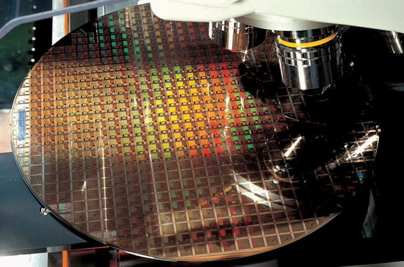
Semiconductor manufacturing milestones rarely arrive without fierce industrial competition, but recent fabrication data emerging from Hsinchu indicates a notable shift in leading-edge logic production. TSMC's transition to Gate-All-Around Field-Effect Transistor (GAAFET) architecture, designated as the N2 process node, has crossed a critical threshold in commercial viability. According to foundry engineering reports reviewed ahead of commercial tape-outs, initial multi-project wafer runs have achieved defect densities significantly lower than those recorded during the early ramp-up of the 3nm FinFET architecture.
The core engineering breakthrough centers on the
The core engineering breakthrough centers on the perfection of nanosheet transistor geometry. By replacing traditional fin structures with vertically stacked horizontal silicon nanosheets, TSMC's process engineers have gained unprecedented control over sub-threshold leakage currents while driving operating voltages down. This architectural evolution is particularly vital for hyperscale AI accelerators and high-performance computing (HPC) processors, where thermal dissipation and power density remain the ultimate bottlenecks to sustained performance scaling.
TSMC: Industry analysts note that major fabless
Industry analysts note that major fabless designers—including Apple, AMD, and NVIDIA—have already secured reserved capacity at TSMC's Fab 12 and Fab 20 complexes. However, the complexity of extreme ultraviolet (EUV) lithography integration, especially with the deployment of high-numerical aperture (High-NA EUV) systems for subsequent layer patterning, has required extensive supply chain coordination. Equipment partners such as ASML have stationed dedicated engineering task forces on-site to minimize downtime on twin-scan exposure tools.
Beyond pure transistor density gains, the?
Beyond pure transistor density gains, the economic implications of these stable early yields are profound. Wafer cost per square millimeter at the 2nm node is widely projected to increase relative to mature nodes, making yield optimization the decisive factor for chip designers' profit margins. By achieving stable defect reduction ahead of schedule, TSMC is positioned to absorb the massive capital expenditure of its fab expansions without forcing steep price hikes onto its primary semiconductor customers. As commercial deliveries ramp up toward the final quarter of the year, the semiconductor industry is moving definitively past the FinFET era into a new generation of multi-gate silicon architecture.
"Taiwan Semiconductor Manufacturing Company (TSMC) has successfully stabilized its 2nm GAAFET manufacturing process, reporting initial wafer sorting yields that surpass internal forecasts and outpace previous node introductions at similar lifecycle stages." — EE Times