 AMD
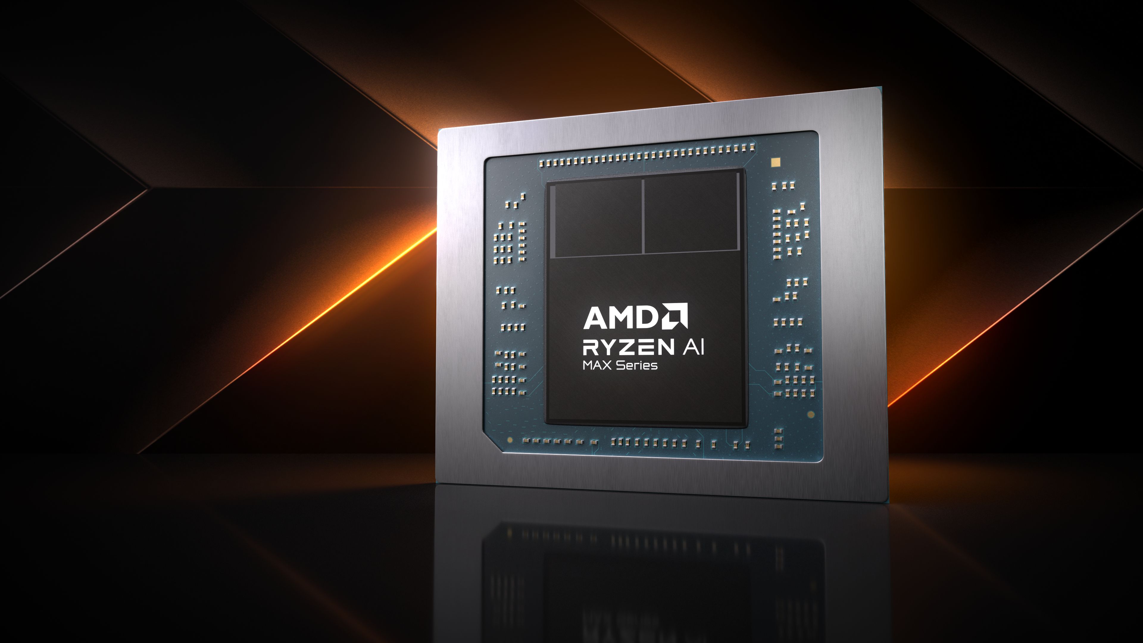
AMDAMD Unveils Multi-Die AI Accelerator Architecture Featuring Advanced Interposer Integration and Liquid Cooling
Advanced Micro Devices has detailed its upcoming enterprise AI processor architecture, utilizing a modular multi-die design and integrated liquid cooling headers to sustain high clock frequencies under continuous datacenter loads.
Explore story →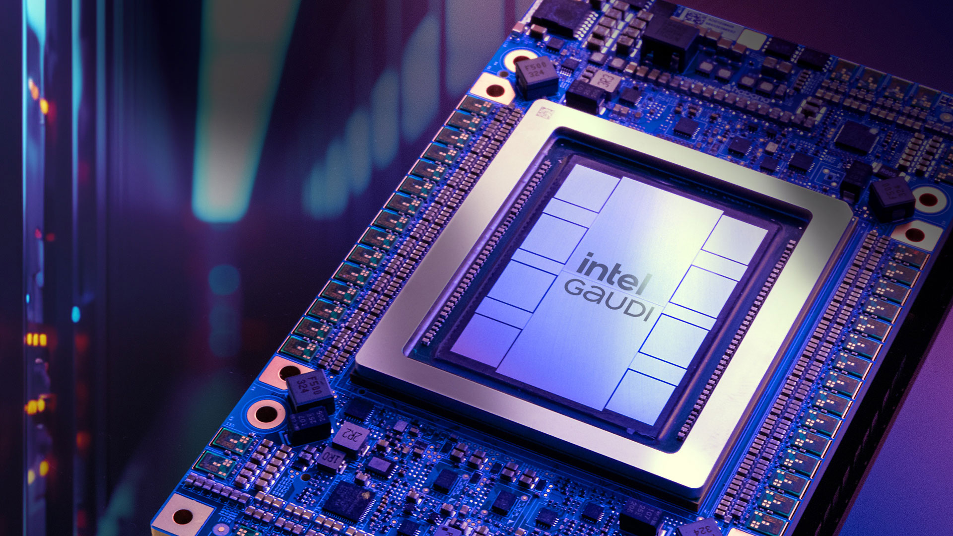 Intel
IntelIntel Pioneers Glass Core Substrate Pilot Line for Next-Generation Multi-Die AI Accelerators
Intel Foundry has advanced its glass core substrate manufacturing initiative into pilot production, offering a viable replacement for organic laminates to eliminate warpage and support ultra-dense multi-chip module packaging.
Explore story →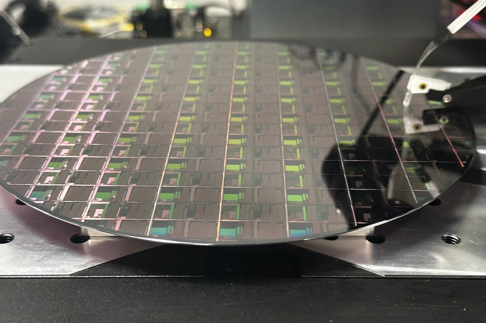 TSMC
TSMCTSMC Integrates Laser Sources Directly onto Silicon Photonics Wafers for Optical Datacenter Links
TSMC has successfully integrated heterogeneous laser diodes directly onto silicon photonics fabrication lines, streamlining the manufacturing of optical transceiver chips for high-speed AI cluster communication.
Explore story →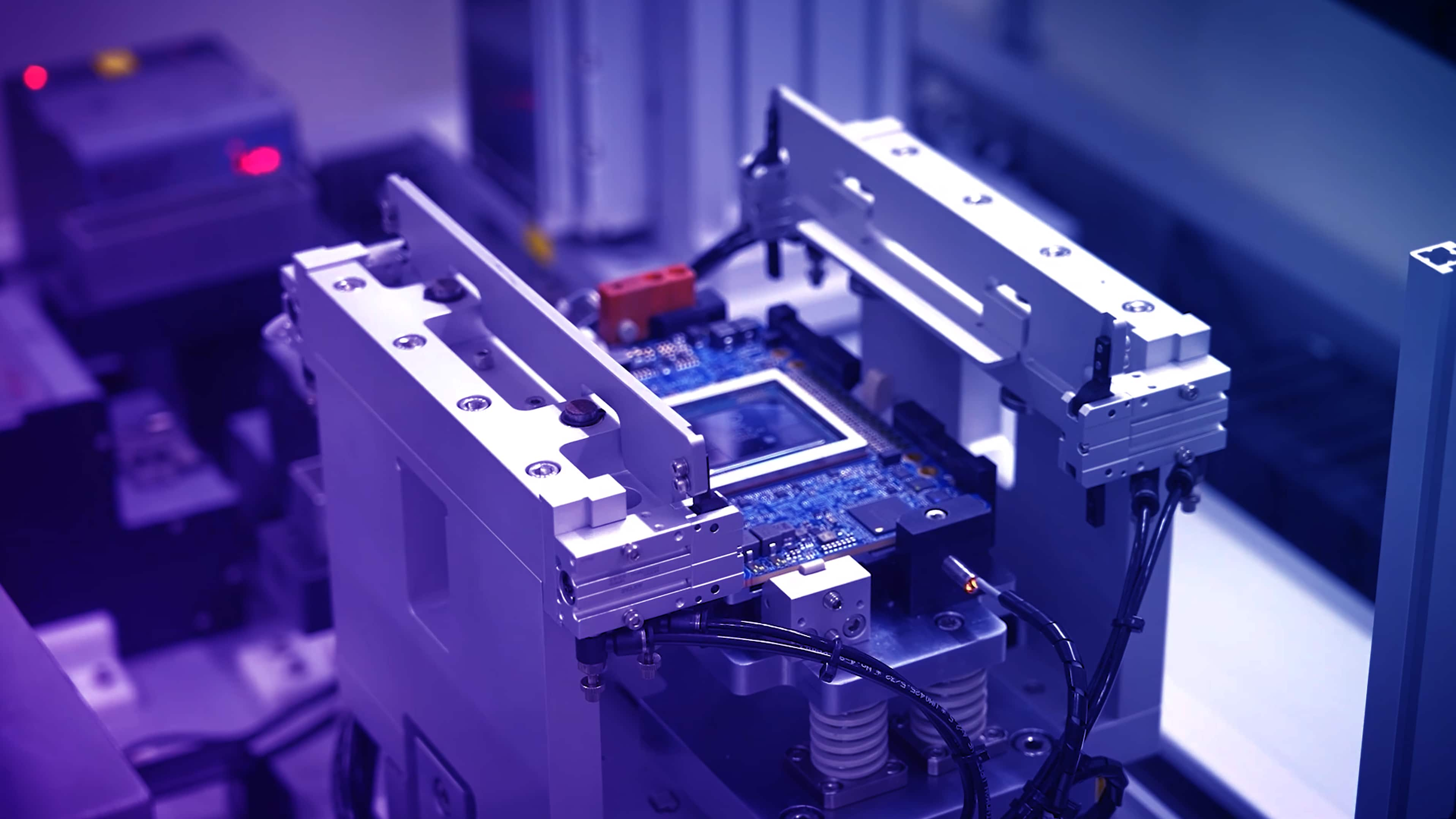 AMD
AMDAdvanced Indium Solder Bonding Techniques Resolve High-Heat Dissipation Challenges in 1000W AI Accelerators
Advanced packaging specialists have perfected controlled indium solder interface bonding methods to maintain structural integrity and low thermal resistance across high-power multi-chip AI processors.
Explore story →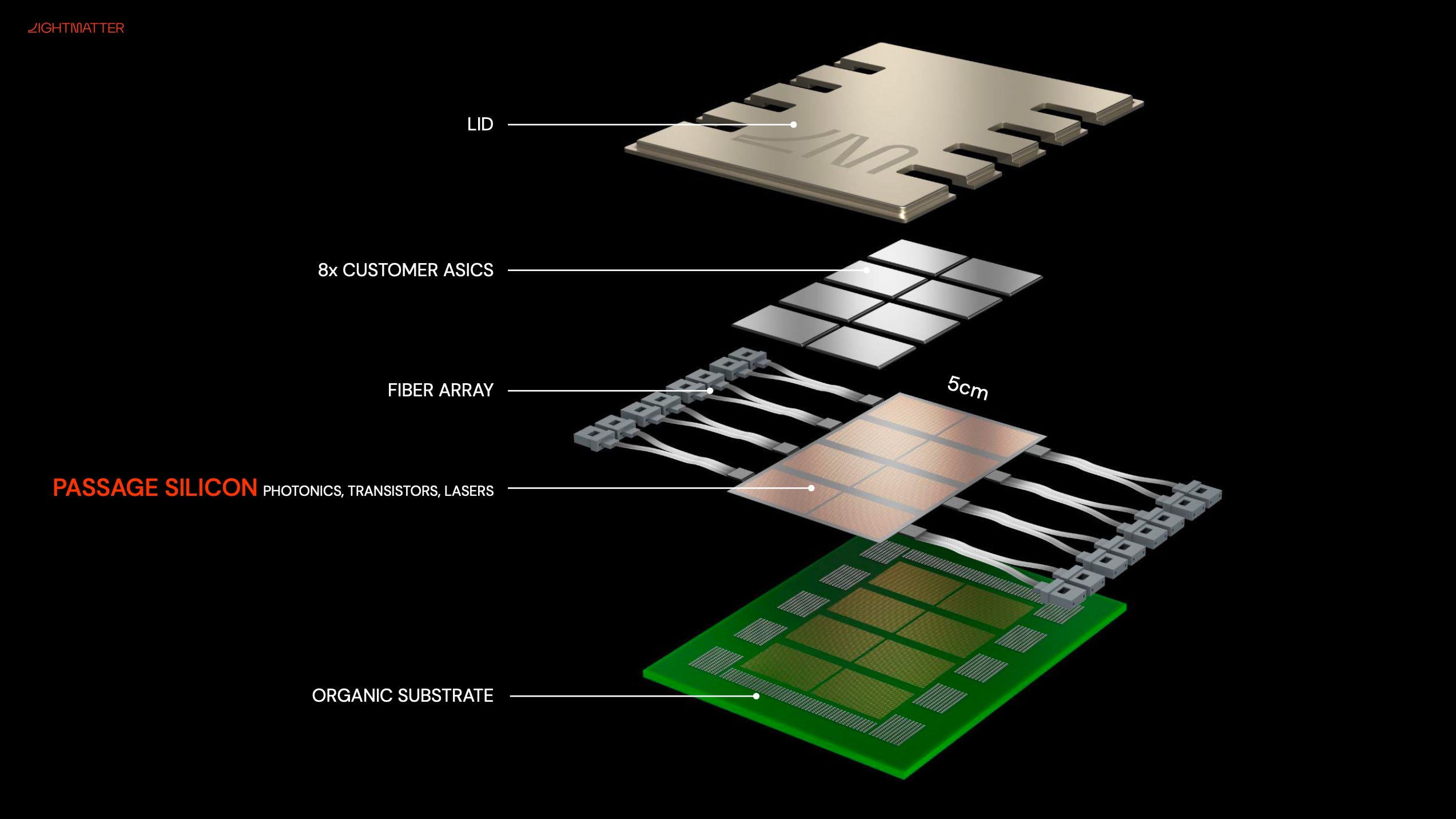 Intel
IntelHigh-Density Silicon Bridge Packaging Eliminates Interposer Bottlenecks in Hyperscale AI Accelerators
Advanced packaging engineers have scaled up embedded multi-die interconnect bridge manufacturing to link multiple compute and memory chiplets without the yield risks of large silicon interposers.
Explore story → AMD
AMDLiquid-Metal Thermal Interface Materials Sustain High Heat Flux in Enterprise AI Workstations
Thermal engineering specialists have qualified gallium-indium liquid metal alloys for mass production, providing superior thermal conductivity for direct-die cooling in enterprise AI hardware.
Explore story → Intel
IntelUCIe Consortium Ratifies Standardized Die-to-Die Protocol for Multi-Vendor Chiplet Ecosystems
The Universal Chiplet Interconnect Express consortium has officially released updated protocol specifications enabling seamless die-to-die communication across disparate foundry nodes.
Explore story → Ayar Labs
Ayar Labs and Enterprise Partners Deploy Optical I/O Chiplets to Break Rack-Level Bandwidth Limits
Optical I/O chiplet architectures are transitioning from research prototypes into commercial data center deployments, replacing high-speed electrical SerDes to link massive AI clusters.
Explore story →ASE Group Expands Panel-Level Packaging Lines for Oversized AI Accelerator Modules
Advanced packaging foundries are ramping up rectangular panel-level packaging capacity to process oversized multi-die substrates more efficiently than traditional round 300mm silicon wafers.
Explore story →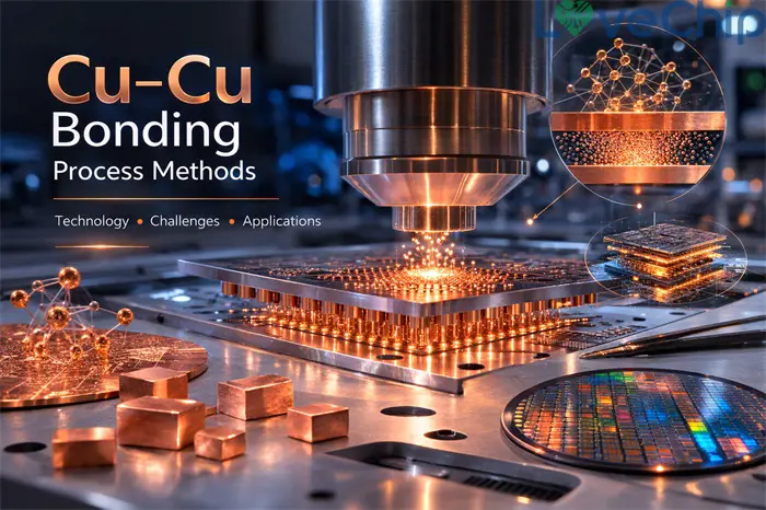 SK Hynix
Direct Cu-Cu Hybrid Bonding Eliminates Micro-Bumps in High-Bandwidth Memory Stacks
Memory manufacturers are deploying direct copper-to-copper hybrid bonding to connect dynamic RAM die layers without solder micro-bumps, reducing vertical profile and thermal resistance.
Explore story →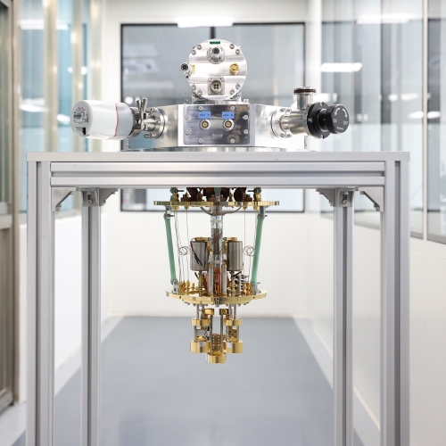 Intel
IntelSuperconducting Single-Photon Detectors Integrated into Silicon Photonic Wafers for Quantum Networks
Researchers have successfully integrated superconducting nanowire single-photon detectors directly onto silicon photonic circuits, advancing scalable optical quantum networking.
Explore story →