 TSMC
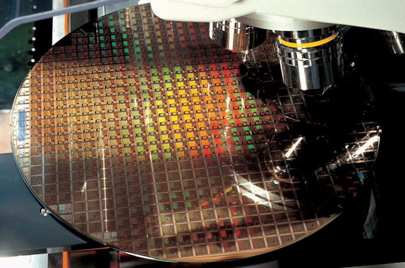
TSMCTSMC 2nm Nanosheet Production Line Achieves Record High Initial Yields Ahead of Major Client Shipments
Taiwan Semiconductor Manufacturing Company (TSMC) has successfully stabilized its 2nm GAAFET manufacturing process, reporting initial wafer sorting yields that surpass internal forecasts and outpace previous node introductions at similar lifecycle stages.
Explore story →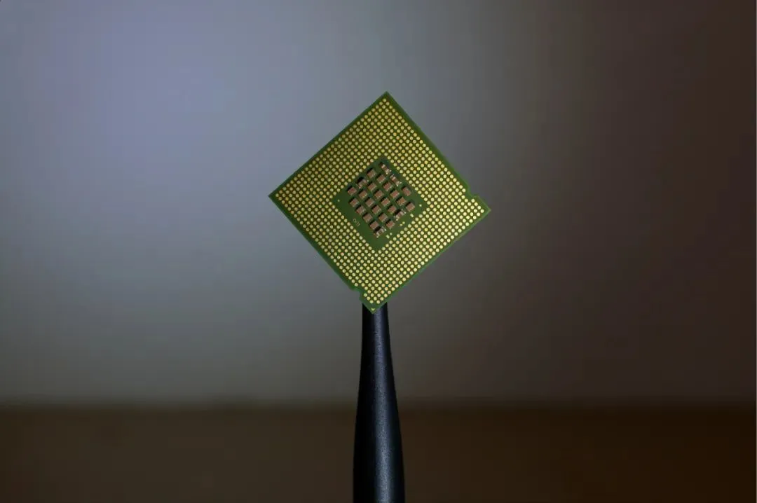 Intel
IntelIntel Foundry Secures Strategic Defense Microelectronics Partnership for Domestic Advanced Packaging
Intel's foundry division has entered into a major multi-year agreement to supply domestic advanced packaging and secure multi-chip module fabrication for critical infrastructure and defense applications.
Explore story → ASML
ASMLASML Ships Next-Generation High-NA EUV Systems to European Research Consortiums for Sub-2nm Lithography Trials
ASML has successfully delivered its latest high-numerical aperture extreme ultraviolet lithography systems to European research facilities, kicking off multi-party collaborative trials for sub-2nm device integration.
Explore story →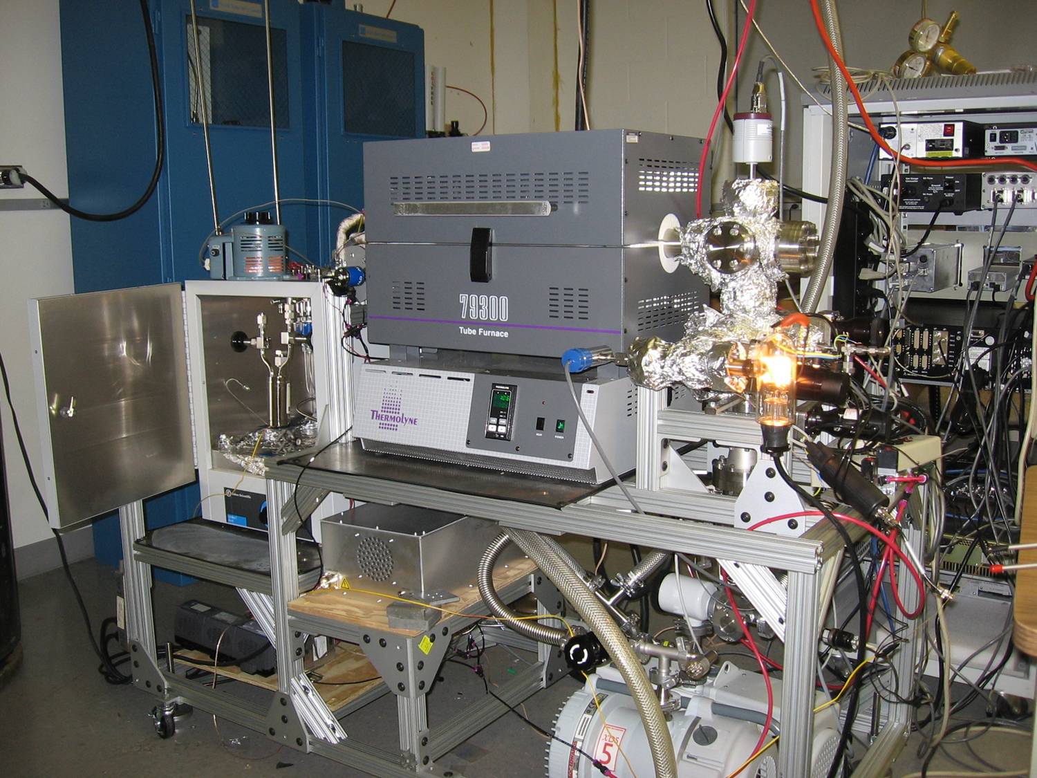 Applied Materials
Applied Materials Introduces Atomic Layer Deposition System for Gate-All-Around Transistor Manufacturing
Applied Materials has announced a specialized atomic layer deposition manufacturing tool designed to deposit uniform dielectric films required for sub-2nm gate-all-around transistor geometries.
Explore story → Samsung
Samsung Electronics Unveils Back-Side Power Delivery Network Strategy for 1.4nm Foundry Node
Samsung Foundry has outlined its technical roadmap for implementing back-side power delivery network technology, aiming to eliminate voltage droop and routing congestion in sub-2nm chip designs.
Explore story →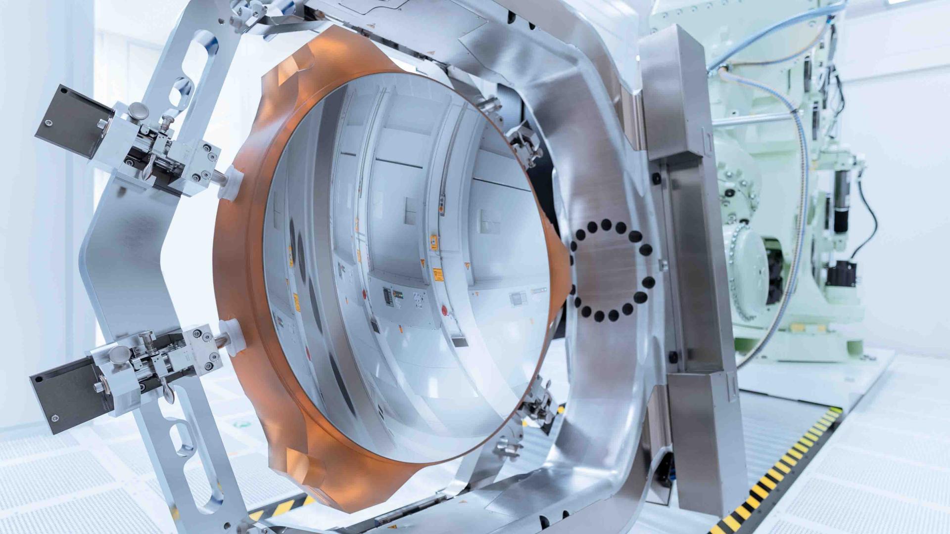 ASML
ASMLASML Validates Carbon Nanotube Pellicles to Protect High-NA EUV Photomasks Under Extreme Thermal Loads
ASML has completed initial durability trials for advanced carbon nanotube pellicle membranes designed to shield extreme ultraviolet photomasks from debris contamination without absorbing excessive exposure energy.
Explore story →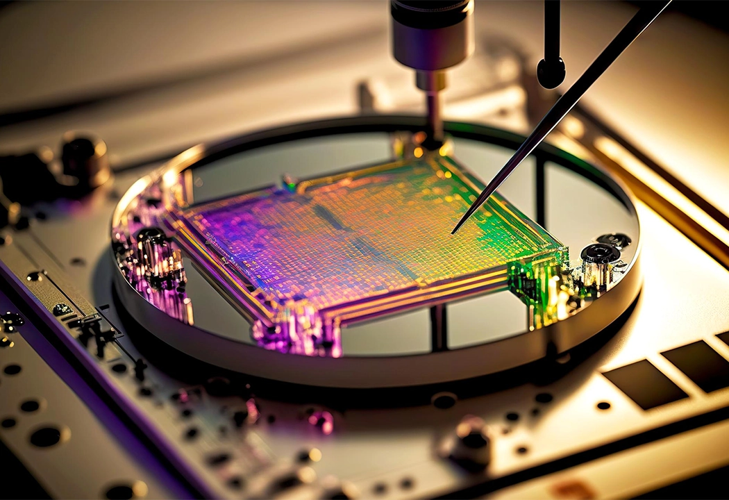 ASML
ASMLExtreme UV Pellicle Optimization Solves Reticle Contamination in High-Volume Sub-2nm Manufacturing
Semiconductor equipment consortia have validated advanced protective pellicle designs that prevent airborne particulate accumulation on EUV photomasks without inducing severe optical energy absorption.
Explore story →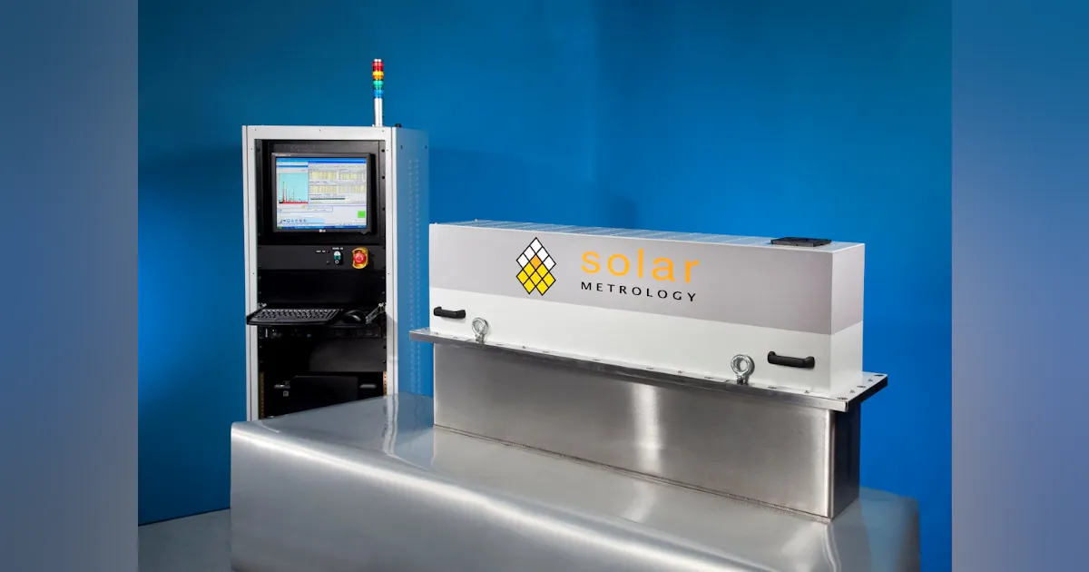 Applied Materials
Advanced Metrology Systems Deploy In-Situ X-Ray Diffraction to Monitor Nanosheet Profile Uniformity
Metrology equipment manufacturers are integrating inline x-ray diffraction inspection tools into advanced fabrication lines to measure atomic-scale structural variations in gate-all-around transistors.
Explore story → Applied Materials
Extreme UV Stochastic Inspection Tools Identify Sub-Nanometer Resist Defects Prior to Etching
Metrology equipment developers have deployed advanced electron-beam and computational inspection platforms designed to detect probabilistic stochastics in extreme ultraviolet photoresists.
Explore story →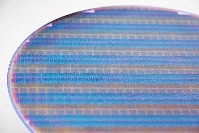 TSMC
TSMCBackside Power Distribution Networks Validate Sub-1.8nm Logic Scaling and Voltage Stability
Leading logic foundries have successfully completed electrical validation test chips utilizing backside power delivery, proving significant reductions in IR drop and signal routing congestion.
Explore story → Lam Research
Atomic Layer Etch Precision Unlocks Damage-Free Gate-All-Around Nanosheet Channel Release
Equipment innovators have refined selective atomic layer etching systems to remove sacrificial silicon-germanium layers cleanly during gate-all-around nanosheet channel release without sidewall damage.
Explore story →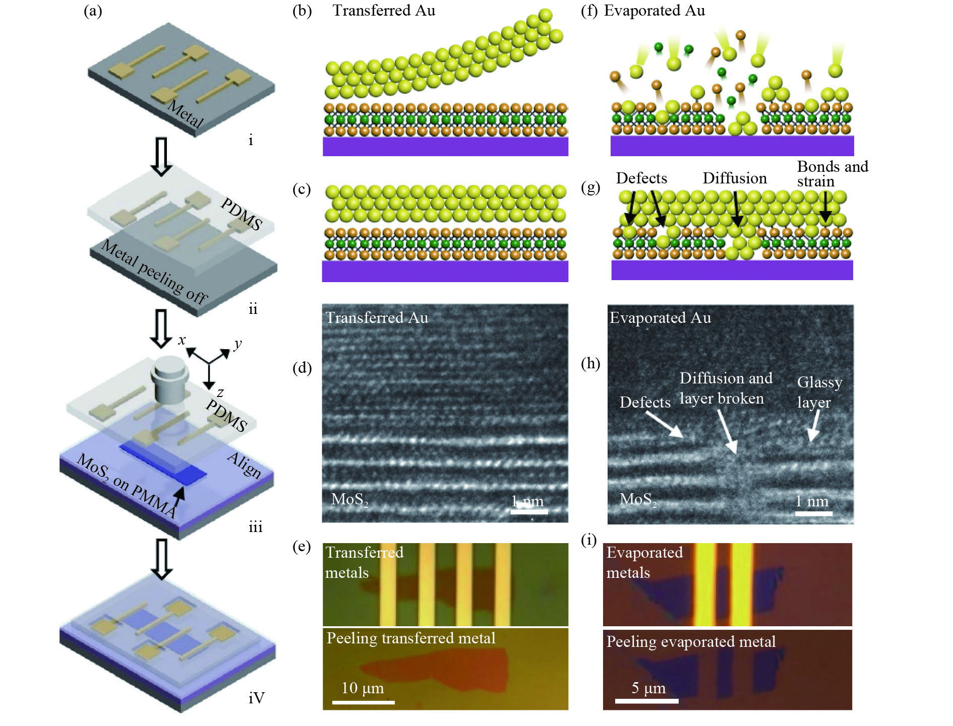 TSMC
TSMCTwo-Dimensional Transition Metal Dichalcogenides Open Path to Sub-1nm Transistor Channels
Researchers have successfully fabricated field-effect transistors using atomic-thin transition metal dichalcogenides, overcoming silicon quantum tunneling limits.
Explore story → ASML
ASMLEUV Reticle Inspection Systems Deploy Multi-Beam Electron Optics for Defect Localization
Advanced mask inspection tools utilizing multi-beam electron optics have entered foundry operation, accelerating defect identification on extreme ultraviolet photomasks.
Explore story →Lasertec Unveils Actinic EUV Patterned Mask Inspection System for Sub-1.5nm Reticles
Advanced metrology equipment manufacturers have introduced actinic extreme ultraviolet patterned mask inspection tools, utilizing 13.5nm light directly to detect subsurface phase defects on sub-1.5nm reticles.
Explore story → imec
imecComplementary FET (CFET) Architecture Achieves Monolithic Vertical Stacking for Sub-1nm Logic
Imec and leading logic foundries have successfully fabricated complementary field-effect transistors, stacking nMOS and pMOS devices vertically to double standard cell layout density.
Explore story → Intel
IntelHigh-NA EUV Lithography Scanners Enter Full-Scale Production Lines for Sub-1.5nm Nodes
Semiconductor foundries have officially integrated high-numerical aperture extreme ultraviolet systems into high-volume manufacturing lines, achieving unprecedented critical dimension control below 1.5nm.
Explore story →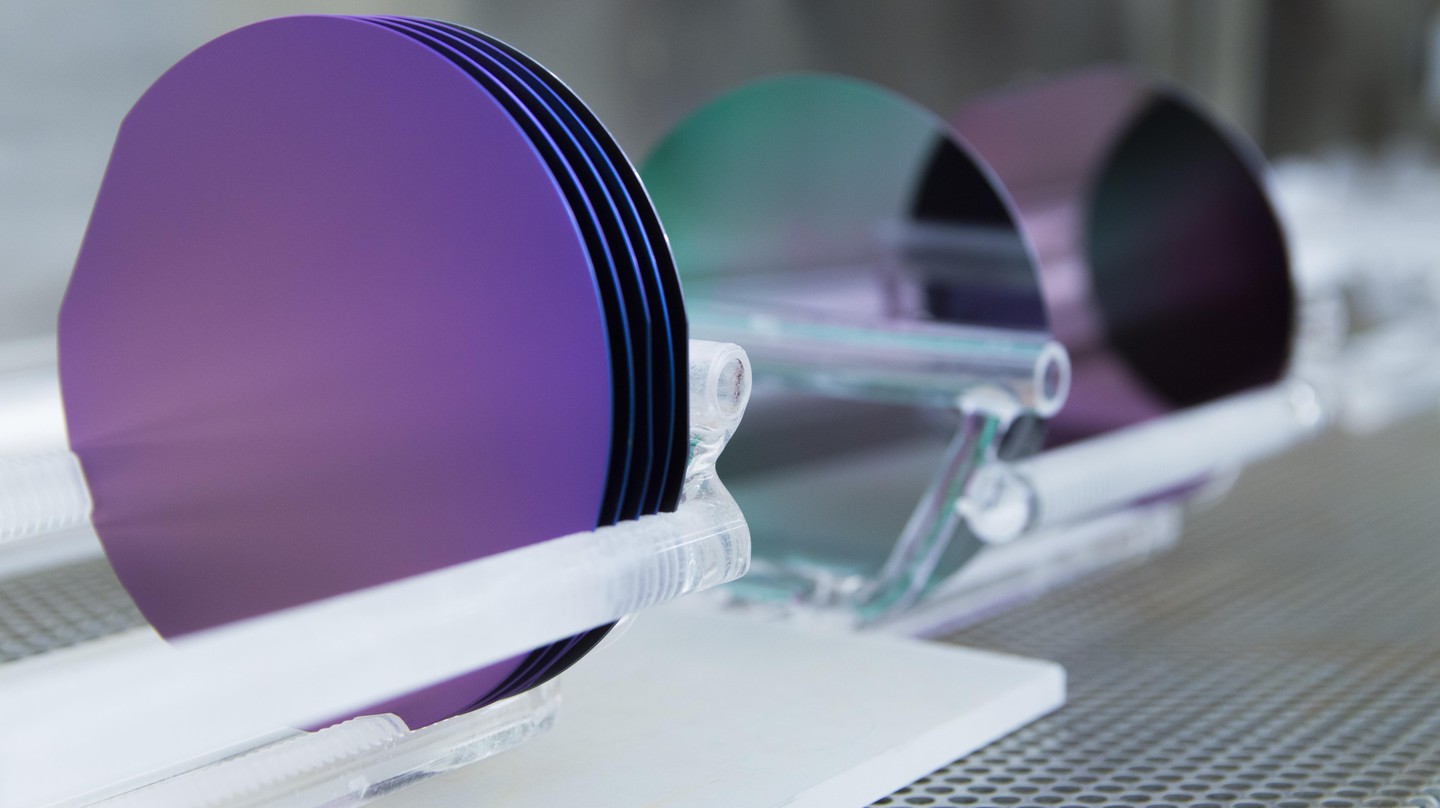 Lam Research
Atomic Layer Deposition Breakthrough Enables Pinpoint High-K Dielectric Uniformity on Nanosheets
Semiconductor equipment developers have refined atomic layer deposition chambers to coat complex gate-all-around nanosheet channels with atomic precision and zero pinhole defects.
Explore story →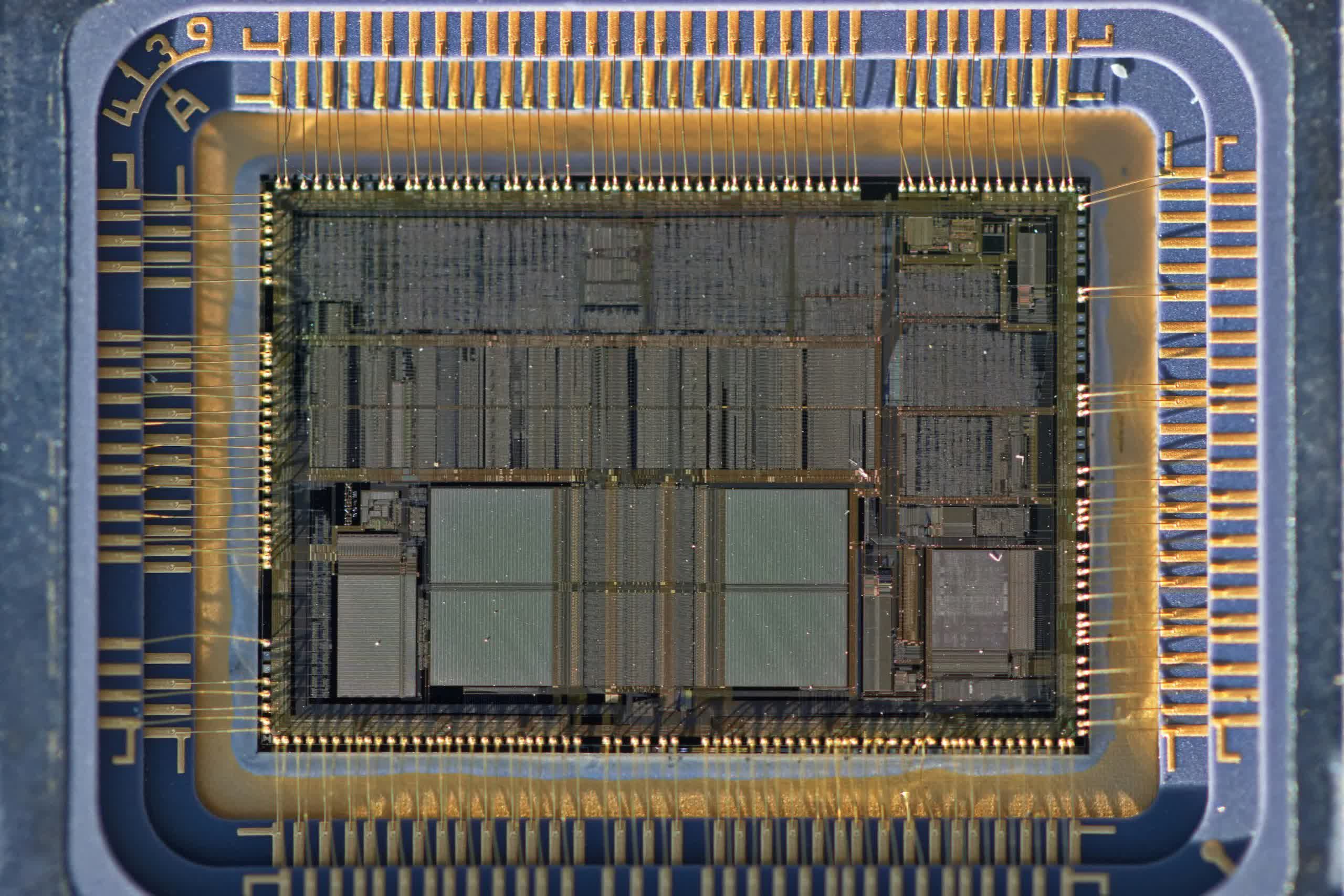 Lam Research
Sub-Nanometer Gate-All-Around Spacer Etch Optimization Enhances Parasitic Capacitance Control
Advanced selective etching systems have mastered inner-spacer recess control for gate-all-around transistors, effectively suppressing parasitic gate-to-source capacitance.
Explore story → Applied Materials
Carbon-Based Interconnect Dielectrics Lower RC Delay in Advanced Backend-of-Line Stacks
Semiconductor materials researchers have validated ultra-low-k carbon-doped dielectric films to minimize signal propagation delays across dense multi-layer copper interconnects.
Explore story →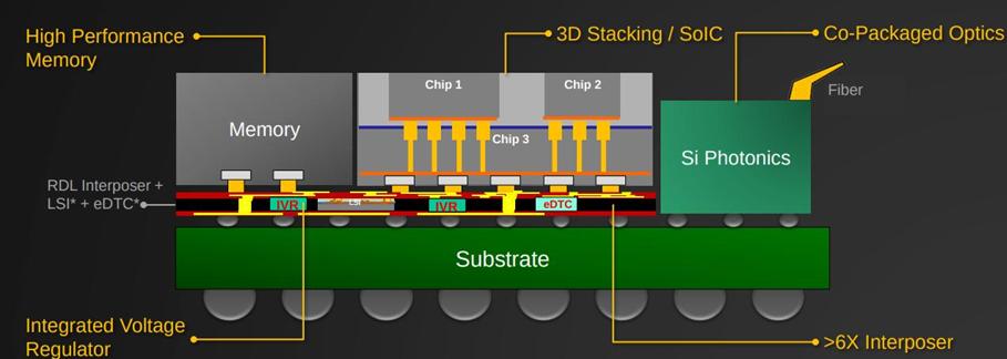 TSMC
TSMCMonolithic 3D Integration Combines Logic and Non-Volatile Memory for Ultra-Dense Edge SoCs
Foundry R&D teams have achieved monolithic three-dimensional stacking of resistive memory directly atop logic circuits, drastically shrinking the footprint of edge intelligence processors.
Explore story →