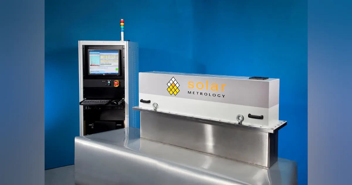
As logic device manufacturing transitions into gate-all-around nanosheet architectures, traditional optical and electron-beam inspection methods are increasingly limited by their inability to accurately probe buried multi-layer structures non-destructively. Inline metrology equipment makers have introduced advanced x-ray diffraction and scattering systems designed to monitor atomic-scale profile uniformity during active wafer fabrication.
The inspection tools utilize high-brilliance x-ray
The inspection tools utilize high-brilliance x-ray sources to penetrate multi-layer gate stacks, capturing detailed diffraction patterns that reveal subtle variations in channel thickness, stress distribution, and compositional profile across 300mm silicon substrates. This high-resolution feedback loop allows process engineers to detect manufacturing anomalies immediately after deposition or etching steps, preventing costly batch scrap events.
Applied Materials: Foundry operators utilizing the metrology
Foundry operators utilizing the metrology systems report tighter control over critical dimension uniformity and improved parametric yields on leading-edge logic nodes. As structural tolerances tighten below the two-nanometer threshold, precise in-situ material characterization plays an indispensable role in maintaining sustainable commercial production volumes.
"Metrology equipment manufacturers are integrating inline x-ray diffraction inspection tools into advanced fabrication lines to measure atomic-scale structural variations in gate-all-around transistors." — IEEE Spectrum