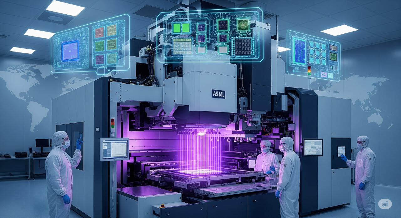
The long-anticipated transition from standard extreme ultraviolet (EUV) lithography to high-numerical aperture (High-NA) systems has shifted from pilot R&D cleanrooms into active high-volume commercial manufacturing lines. Leading semiconductor foundries have completed calibration runs for 0.55 NA lithography equipment, enabling single-exposure pattern printing for critical device layers that previously required complex, yield-limiting multi-patterning techniques.
High-NA EUV systems increase the optical numerical
High-NA EUV systems increase the optical numerical aperture from 0.33 to 0.55, sharpening image contrast and allowing optical elements to resolve finer features directly onto photoresist-coated silicon wafers. However, the anamorphic magnification required by the optical design compresses the field of view in one axis, forcing design rules and reticle layouts to adapt to new stitching and reticle partitioning constraints.
Intel: Foundry lithography teams worked closely
Foundry lithography teams worked closely with equipment manufacturers to refine anamorphic mask tooling, specialized photoresists, and ultra-thin pellicle membranes capable of withstanding the intense photon flux of high-power plasma sources. Early yield telemetry confirms that single-exposure High-NA patterning reduces edge placement error variance and significantly shortens cycle times compared to quadruple-patterning DUV or multi-exposure standard EUV flows.
The successful operational deployment of High-NA?
The successful operational deployment of High-NA EUV marks a pivotal milestone for the semiconductor industry, securing optical lithography's viability as the primary scaling engine for sub-1.5nm logic and memory manufacturing.
Key Takeaways
- Intel continues to push boundaries in lithography equipment.
- The development addresses fundamental physical limitations in semiconductor scaling.
- Commercial viability will depend on yield stability and supply chain integration.