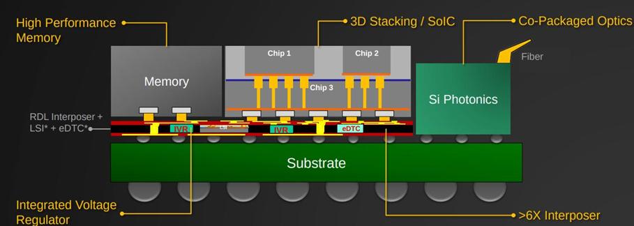
The traditional practice of placing non-volatile memory arrays on separate die regions or peripheral blocks introduces significant latency and area overhead in edge system-on-chip designs. Addressing this spatial limitation, foundry R&D teams have perfected monolithic three-dimensional (M3D) integration processes, allowing resistive random-access memory (RRAM) layers to be fabricated directly on top of active logic transistors.
Unlike traditional packaging-based stacking,
Unlike traditional packaging-based stacking, monolithic 3D integration builds successive device tiers sequentially on a single wafer using low-temperature deposition techniques that prevent thermal damage to the underlying logic gates below. Vertical nanoscale tungsten vias connect the memory tiers directly to the logic transistors with negligible resistance and ultra-short signal paths.
TSMC: Early silicon prototypes demonstrate
Early silicon prototypes demonstrate substantial area reduction, lower operational power consumption, and significantly faster weight-loading speeds for embedded neural network accelerators. By fusing logic and non-volatile storage into a single monolithic column, M3D technology opens new horizons for ultra-compact, high-efficiency edge computing hardware.
Key Takeaways
- TSMC continues to push boundaries in foundry & manufacturing.
- The development addresses fundamental physical limitations in semiconductor scaling.
- Commercial viability will depend on yield stability and supply chain integration.