 Applied Materials
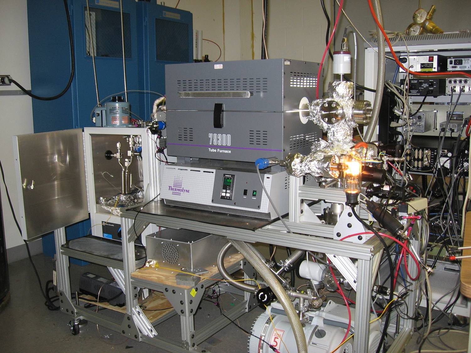
Applied Materials Introduces Atomic Layer Deposition System for Gate-All-Around Transistor Manufacturing
Applied Materials has announced a specialized atomic layer deposition manufacturing tool designed to deposit uniform dielectric films required for sub-2nm gate-all-around transistor geometries.
Read briefing →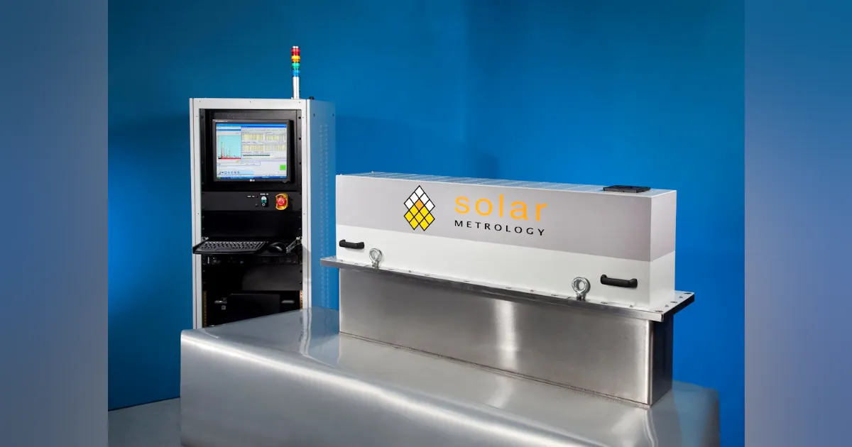 Applied Materials
Advanced Metrology Systems Deploy In-Situ X-Ray Diffraction to Monitor Nanosheet Profile Uniformity
Metrology equipment manufacturers are integrating inline x-ray diffraction inspection tools into advanced fabrication lines to measure atomic-scale structural variations in gate-all-around transistors.
Read briefing → Applied Materials
Extreme UV Stochastic Inspection Tools Identify Sub-Nanometer Resist Defects Prior to Etching
Metrology equipment developers have deployed advanced electron-beam and computational inspection platforms designed to detect probabilistic stochastics in extreme ultraviolet photoresists.
Read briefing → Lam Research
Atomic Layer Etch Precision Unlocks Damage-Free Gate-All-Around Nanosheet Channel Release
Equipment innovators have refined selective atomic layer etching systems to remove sacrificial silicon-germanium layers cleanly during gate-all-around nanosheet channel release without sidewall damage.
Read briefing → ASML
ASMLEUV Reticle Inspection Systems Deploy Multi-Beam Electron Optics for Defect Localization
Advanced mask inspection tools utilizing multi-beam electron optics have entered foundry operation, accelerating defect identification on extreme ultraviolet photomasks.
Read briefing →Lasertec Unveils Actinic EUV Patterned Mask Inspection System for Sub-1.5nm Reticles
Advanced metrology equipment manufacturers have introduced actinic extreme ultraviolet patterned mask inspection tools, utilizing 13.5nm light directly to detect subsurface phase defects on sub-1.5nm reticles.
Read briefing →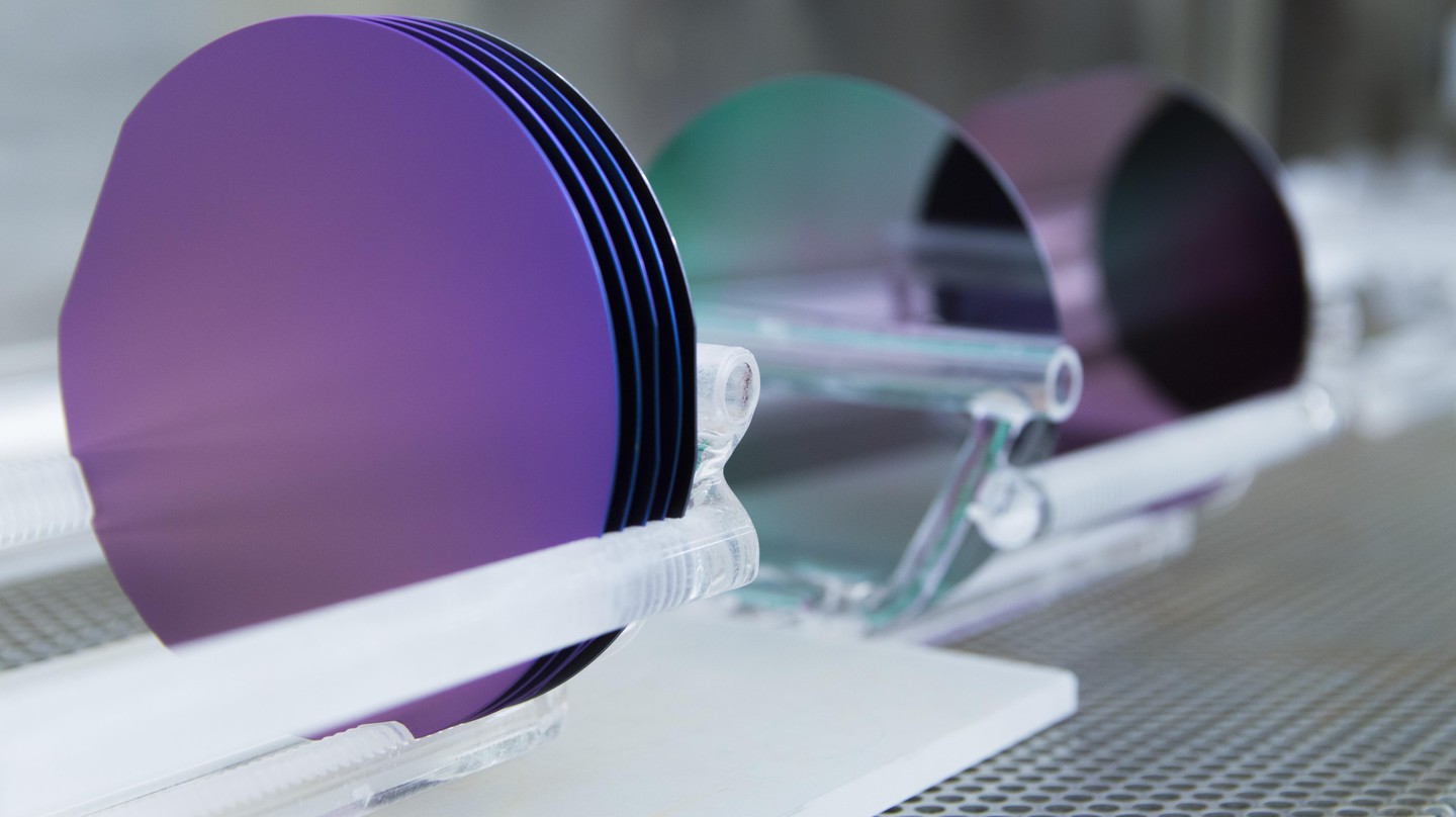 Lam Research
Atomic Layer Deposition Breakthrough Enables Pinpoint High-K Dielectric Uniformity on Nanosheets
Semiconductor equipment developers have refined atomic layer deposition chambers to coat complex gate-all-around nanosheet channels with atomic precision and zero pinhole defects.
Read briefing →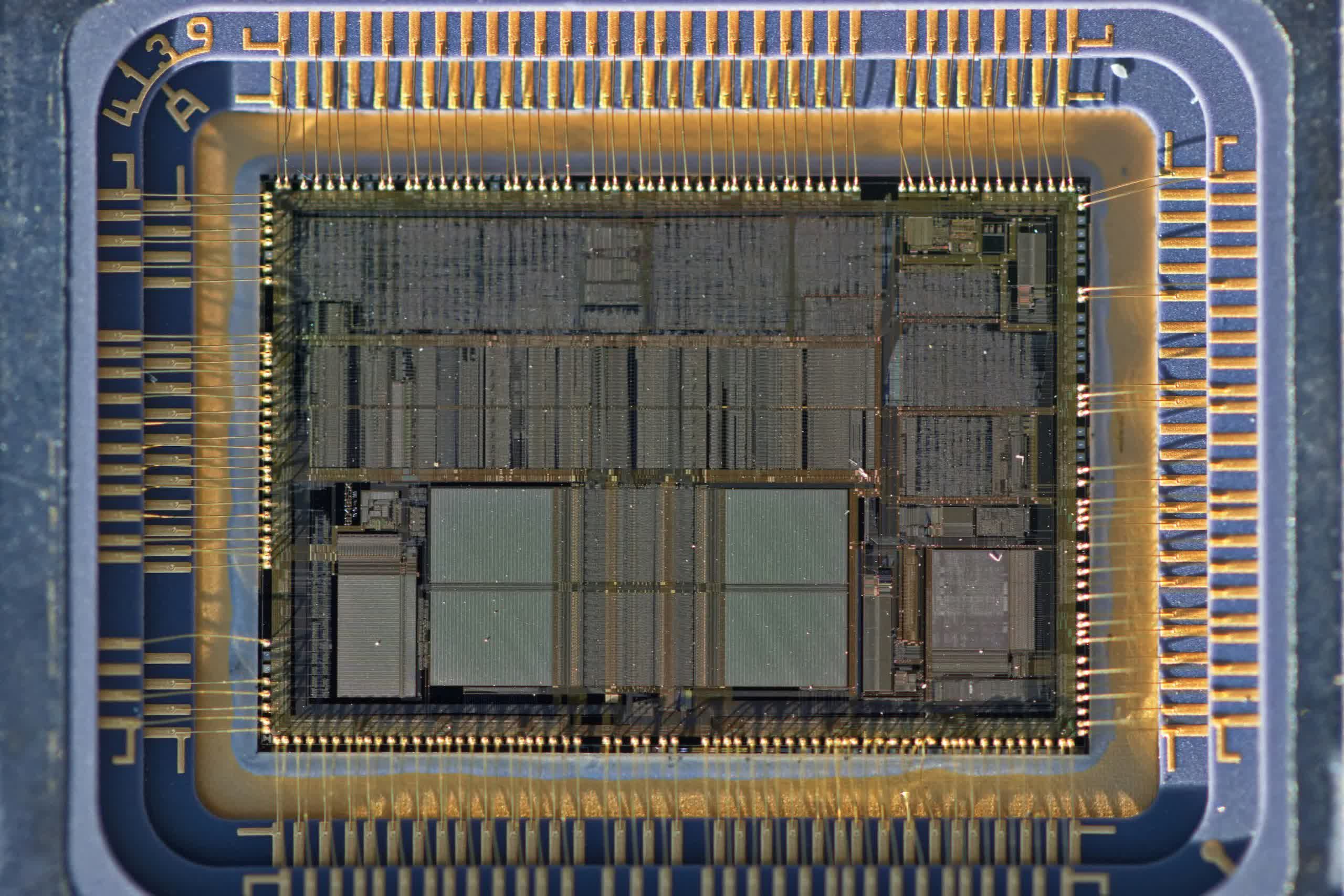 Lam Research
Sub-Nanometer Gate-All-Around Spacer Etch Optimization Enhances Parasitic Capacitance Control
Advanced selective etching systems have mastered inner-spacer recess control for gate-all-around transistors, effectively suppressing parasitic gate-to-source capacitance.
Read briefing →