What follows is a closer look at extreme uv stochastic inspection tools identify sub-nanometer resist defects prior to etching — not as a product announcement, but as an engineering story with real consequences for the semiconductor supply chain.
As lithography processes push deeper into sub-2nm
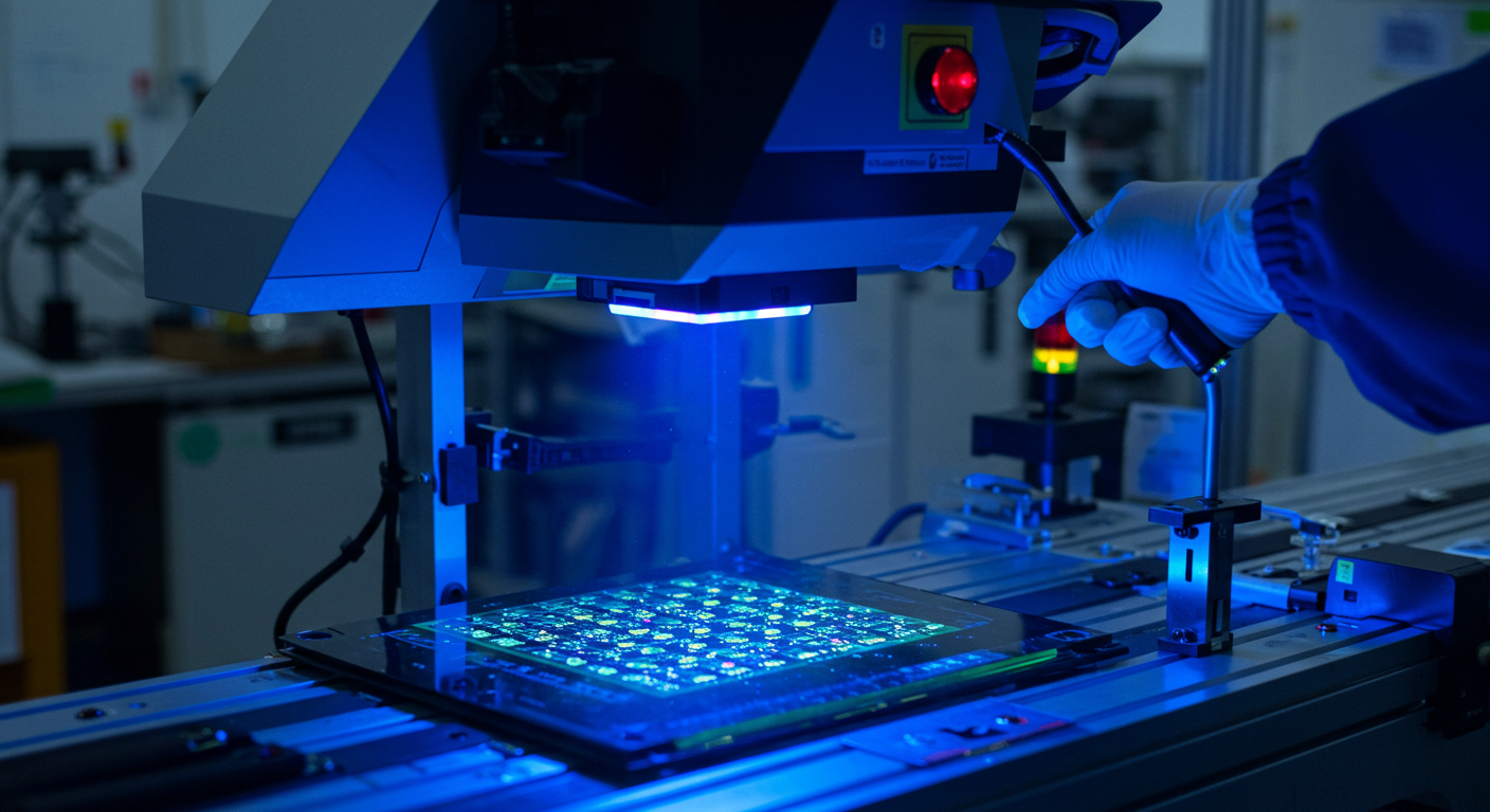
As lithography processes push deeper into sub-2nm dimensions using extreme ultraviolet (EUV) exposure systems, physical phenomena known as stochastics present a severe threat to manufacturing yields. Because EUV photons carry high energy but low overall particle density per unit area, random statistical variations in photon arrival times can cause localized under-exposure or bridging defects within photoresist films. To combat this microscopic unpredictability, advanced metrology equipment manufacturers have introduced high-speed inspection platforms equipped with computational stochastic analysis software.
The newly deployed inspection tools utilize
The newly deployed inspection tools utilize high-resolution electron beams combined with machine learning classification algorithms to scan patterned wafers immediately after development. Instead of searching merely for macro-scale pattern bridging or breaks, the software analyzes line-edge roughness and local critical dimension uniformity across billions of individual transistor gate structures.
Applied Materials: Process engineers utilize the rapid feedback
Process engineers utilize the rapid feedback data to fine-tune photoresist chemical compositions, post-exposure bake temperatures, and scanner illumination dose parameters in real-time. This proactive adjustment capability prevents defective wafers from proceeding down the manufacturing line to expensive dry etching and metal deposition stages.
Foundry operations implementing stochastic?
Foundry operations implementing stochastic inspection report meaningful improvements in parametric yield stability on advanced logic nodes. As feature sizes shrink to dimensions where individual molecular variations alter electrical behavior, advanced metrology remains an essential line of defense for commercial semiconductor fabrication.