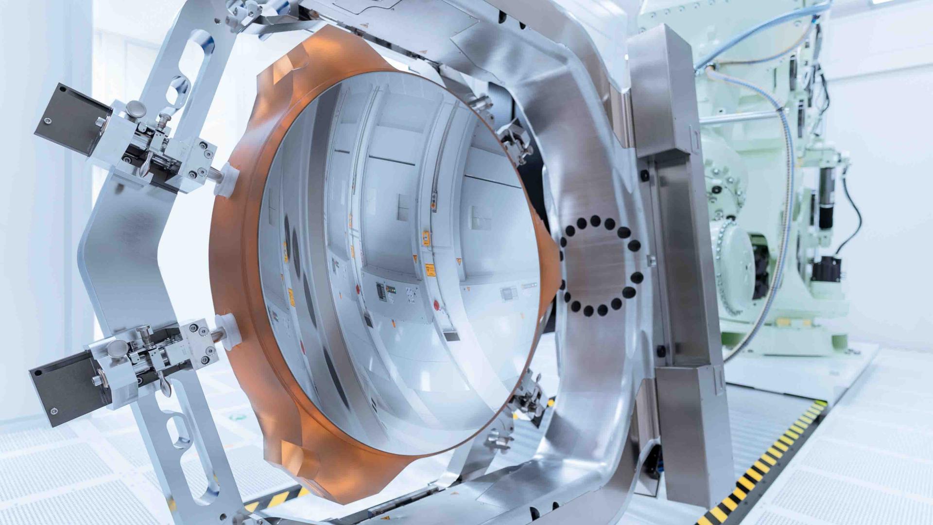
The deployment of high-numerical aperture (High-NA) extreme ultraviolet (EUV) lithography systems has brought forth severe material science challenges, particularly regarding the preservation of expensive photomasks during high-power exposure runs. ASML has successfully finalized structural durability validation for a new class of carbon nanotube (CNT) pellicle membranes engineered to protect patterned reticles from airborne particle deposition without causing unacceptable optical transmission loss.
In standard EUV lithography operating at 13
In standard EUV lithography operating at 13.5nm wavelengths, traditional polysilicon or metallic pellicle films absorb significant amounts of incoming photon energy, resulting in extreme thermal stress that can warp the membrane or degrade image contrast on the silicon wafer. Because High-NA systems utilize higher power plasma sources to maximize throughput, pellicle survivability under intense thermal radiation has become a critical gating factor for commercial yield stability.
ASML: The newly validated carbon nanotube pellicle
The newly validated carbon nanotube pellicle features a highly porous, single-walled network architecture that permits exceptional EUV transmission efficiency exceeding ninety percent while maintaining high mechanical tensile strength. The open-mesh physical structure allows scattered gas molecules to pass through freely, preventing pressure differentials across the membrane during rapid vacuum chamber pressure cycling.
Mask shop operations and foundry lithography?
Mask shop operations and foundry lithography teams have begun incorporating the CNT pellicles into pilot exposure runs for sub-2nm device layers. Preliminary data confirms that the membranes withstand high-intensity photon bombardment over extended operational shifts without sagging or structural degradation, ensuring consistent critical dimension uniformity across mass-produced silicon wafers.
Key Takeaways
- ASML continues to push boundaries in lithography equipment.
- The development addresses fundamental physical limitations in semiconductor scaling.
- Commercial viability will depend on yield stability and supply chain integration.