The semiconductor industry is entering an era in which the most important breakthroughs are often hidden inside the layers between a transistor and a finished system. This briefing examines what this development means, why it matters now, and which signals will determine its lasting value.
The structural evolution of logic semiconductor fabrication
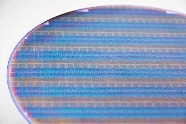
The structural evolution of logic semiconductor fabrication has reached a defining architectural junction with the physical separation of power delivery and signal routing networks. Leading logic foundries have concluded initial electrical characterization of test chips featuring Backside Power Distribution Network (BSPDN) architecture, confirming that routing power rails to the reverse side of thinned silicon wafers successfully eliminates voltage droop and metal layer congestion.
In traditional transistor layouts, power distribution
In traditional transistor layouts, power distribution lines and high-speed data signals share the upper metal interconnect layers on the front side of the die. As transistor gate pitches shrink below two nanometers, these shared metal layers become severely congested, leading to high electrical resistance, increased RC signal delay, and significant voltage drop across the active processor core.
TSMC: BSPDN resolves this physical bottleneck by
BSPDN resolves this physical bottleneck by relocating power delivery lines entirely to the back of the silicon substrate, connecting them directly to the active transistor source and drain terminals through microscopic through-silicon vias. This decoupling frees up the entire front-side metal stack exclusively for signal interconnects, enabling denser standard cell library layouts and shorter wire lengths.
Electrical telemetry from test wafer runs?
Electrical telemetry from test wafer runs indicates substantial reductions in power distribution resistance and improved operating voltage stability under peak transient current spikes. As the industry transitions toward sub-1.8nm production nodes, backside power delivery is firmly established as a mandatory structural foundation for high-performance microprocessors.