The semiconductor industry is entering an era in which the most important breakthroughs are often hidden inside the layers between a transistor and a finished system. This briefing examines what this development means, why it matters now, and which signals will determine its lasting value.
As traditional bulk silicon channels approach physical
As traditional bulk silicon channels approach physical thickness limits where quantum mechanical tunneling causes severe off-state leakage currents, materials science teams are exploring alternative semiconductor channels. A collaborative research initiative involving leading foundry scientists has successfully demonstrated functional field-effect transistors utilizing monolayer transition metal dichalcogenides (TMDs) as the primary channel material.
Unlike silicon, which requires a finite thickness to
Unlike silicon, which requires a finite thickness to maintain electronic mobility, TMD materials such as molybdenum disulfide can maintain robust semiconducting properties at thicknesses of just three atoms. This atomic thinness allows gate electrodes to exert absolute electrostatic control over the channel, effectively suppressing short-channel effects and sub-threshold leakage down to sub-one-nanometer gate lengths.
TSMC: The primary engineering hurdle overcome
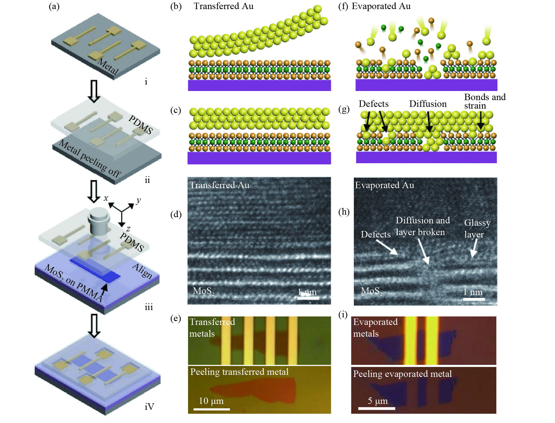
The primary engineering hurdle overcome during the fabrication trials involved developing low-resistance metal contacts that do not Fermi-pin or chemically damage the fragile 2D sheet. Utilizing specialized van der Waals contact integration techniques, the team achieved clean electrical interfaces without introducing crystalline defects.
While commercial high-volume manufacturing of?
While commercial high-volume manufacturing of TMD-based logic remains years away, this breakthrough confirms that post-silicon material channels can theoretically sustain transistor scaling long after conventional silicon scaling runs its course.