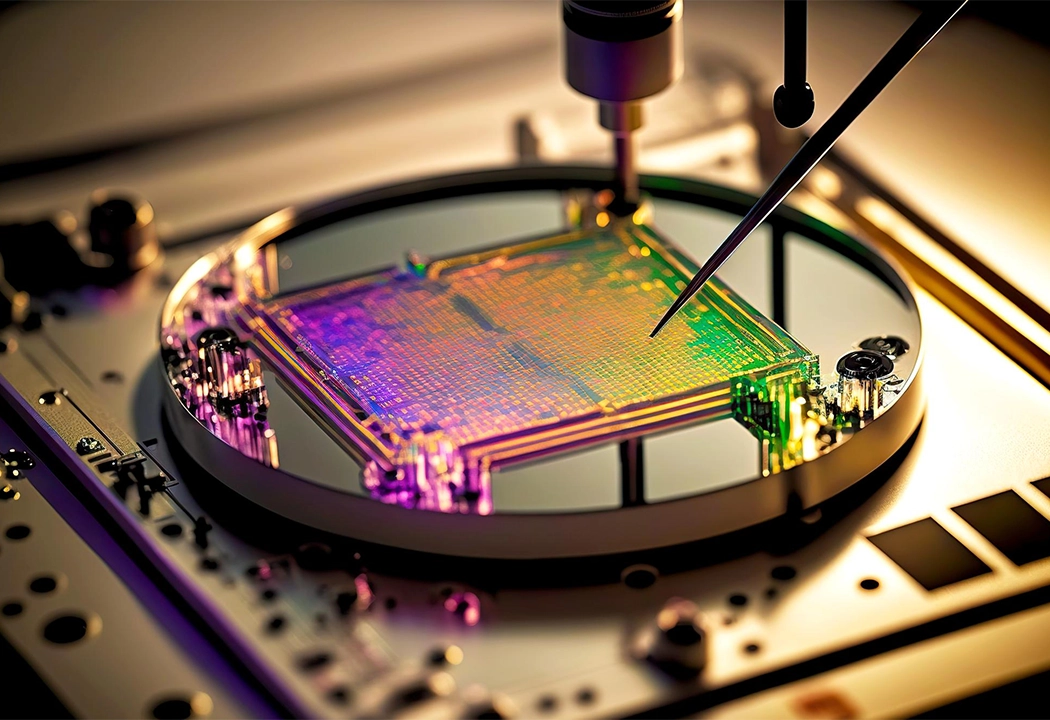
Maintaining absolute surface cleanliness on extreme ultraviolet (EUV) photomasks is a primary determinant of wafer yield in leading-edge logic fabrication. As foundries ramp up production on sub-2nm nodes, exposure to higher EUV source power levels increases the risk of reticle damage caused by stray debris and outgassed chemical residues within the lithography scanner chamber. Equipment engineering teams have successfully optimized advanced protective pellicle membranes designed to shield patterned reticles without compromising exposure precision.
The core challenge in EUV pellicle design stems from
The core challenge in EUV pellicle design stems from the 13.5nm wavelength's tendency to be absorbed by most conventional materials, leading to extreme thermal distortion and loss of optical throughput. The newly validated pellicle utilizes ultra-thin carbon-based composite structures that maintain high optical transparency while withstanding intense photon bombardment over prolonged operational cycles.
ASML: Foundry integration specialists note that
Foundry integration specialists note that the implementation of these robust pellicles significantly extends photomask lifespans and reduces the frequency of cleaning interventions required during high-volume manufacturing runs. This reliability improvement is essential for keeping fabrication lines operating at optimal throughput and minimizing production costs for fabless semiconductor designers.
Key Takeaways
- ASML continues to push boundaries in lithography equipment.
- The development addresses fundamental physical limitations in semiconductor scaling.
- Commercial viability will depend on yield stability and supply chain integration.