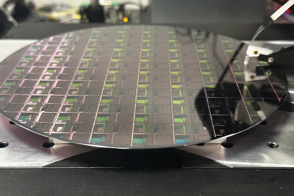
The transition from electrical copper interconnects to optical communications within massive artificial intelligence training clusters has long been hindered by manufacturing complexity, particularly the challenge of coupling external laser light sources onto silicon photonic integrated circuits. Taiwan Semiconductor Manufacturing Company (TSMC) has addressed this fundamental hurdle by deploying a manufacturing process that integrates III-V semiconductor laser diodes directly onto standard silicon photonic wafers at scale.
such as indium phosphide
Historically, optical transceivers required separate manufacturing paths where III-V optical gain materials—such as indium phosphide—were individually aligned and bonded onto silicon substrates using cumbersome pick-and-place packaging tools. This manual or semi-automated assembly step introduced high optical coupling losses, assembly variance, and high unit costs. TSMC’s new integration methodology utilizes advanced wafer-scale bonding and selective epitaxial growth, enabling laser sources to be embedded directly into designated optical cavities during the primary fabrication sequence.
TSMC: The process engineering required precise
The process engineering required precise control over lattice mismatch between silicon and III-V compound semiconductor materials to prevent dislocation defects that degrade laser efficiency and operational lifetime. By utilizing proprietary buffer layers and localized thermal annealing techniques, foundry engineers achieved stable continuous-wave laser emission across standardized optical wavelengths directly from the host silicon wafer.
Datacenter infrastructure architects anticipate?
Datacenter infrastructure architects anticipate that wafer-level laser integration will drastically reduce the cost and physical footprint of optical transceivers utilized in co-packaged optics architectures. As training clusters scale beyond tens of thousands of accelerator nodes, reliable optical interconnect manufacturing ensures that data transmission bandwidth keeps pace with raw computational capacity.
"TSMC has successfully integrated heterogeneous laser diodes directly onto silicon photonics fabrication lines, streamlining the manufacturing of optical transceiver chips for high-speed AI cluster communication." — SemiAnalysis