 Intel
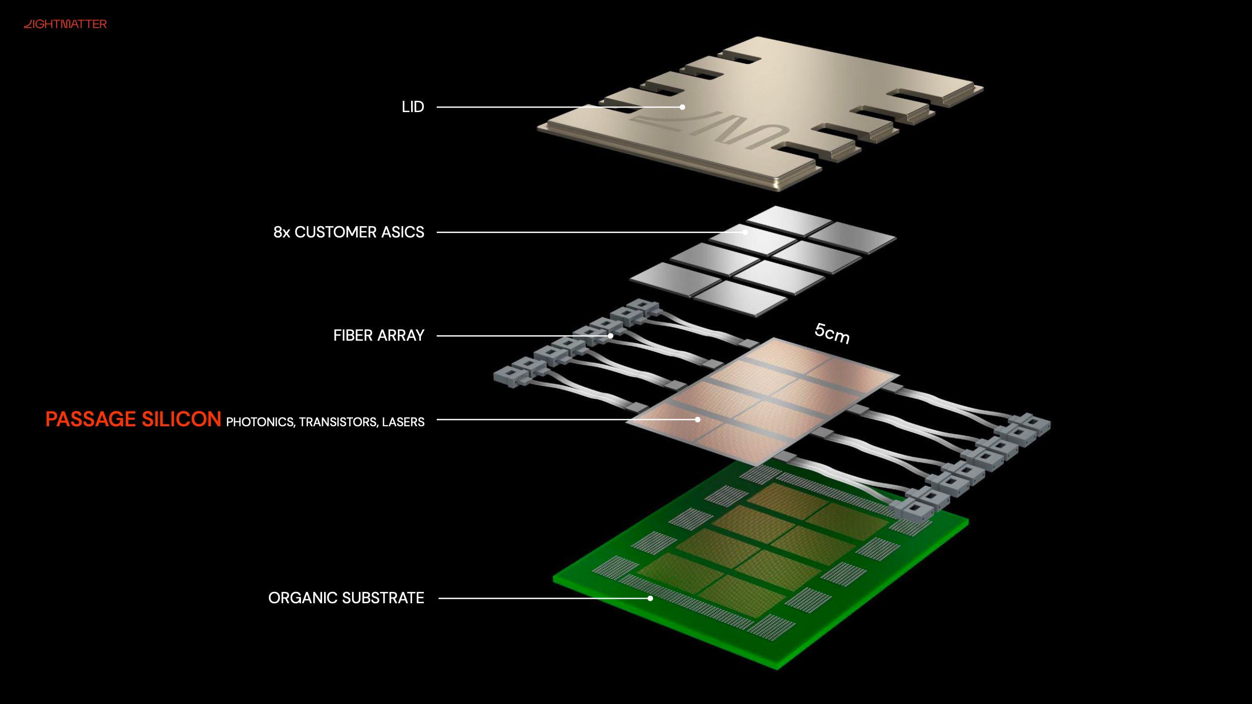
IntelHigh-Density Silicon Bridge Packaging Eliminates Interposer Bottlenecks in Hyperscale AI Accelerators
Advanced packaging engineers have scaled up embedded multi-die interconnect bridge manufacturing to link multiple compute and memory chiplets without the yield risks of large silicon interposers.
Read briefing → Intel
IntelUCIe Consortium Ratifies Standardized Die-to-Die Protocol for Multi-Vendor Chiplet Ecosystems
The Universal Chiplet Interconnect Express consortium has officially released updated protocol specifications enabling seamless die-to-die communication across disparate foundry nodes.
Read briefing →ASE Group Expands Panel-Level Packaging Lines for Oversized AI Accelerator Modules
Advanced packaging foundries are ramping up rectangular panel-level packaging capacity to process oversized multi-die substrates more efficiently than traditional round 300mm silicon wafers.
Read briefing →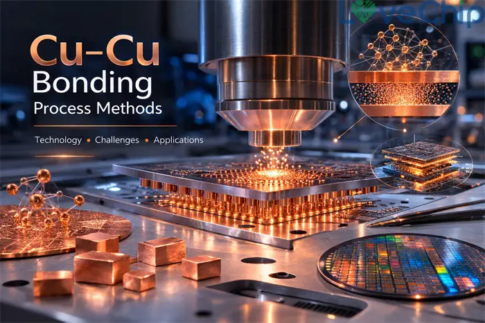 SK Hynix
Direct Cu-Cu Hybrid Bonding Eliminates Micro-Bumps in High-Bandwidth Memory Stacks
Memory manufacturers are deploying direct copper-to-copper hybrid bonding to connect dynamic RAM die layers without solder micro-bumps, reducing vertical profile and thermal resistance.
Read briefing →