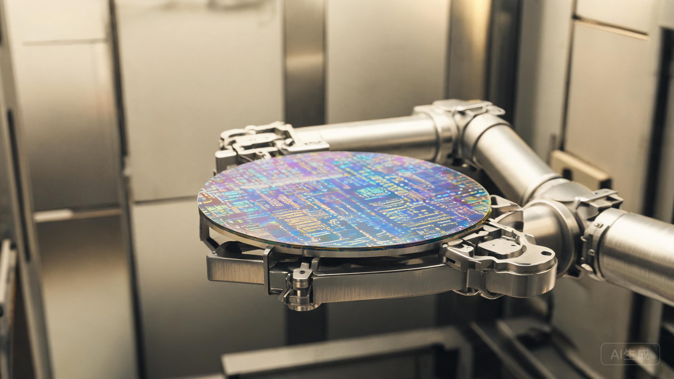
What follows is a closer look at tsmc a16 hits volume production: backside power delivery moves from roadmap to revenue — not as a product announcement, but as an engineering story with real consequences for the semiconductor supply chain.
TSMC has begun high-volume manufacturing on A16, the node
TSMC has begun high-volume manufacturing on A16, the node it positions as the first production process to combine nanosheet transistors with a complete backside power delivery network. Wafers are now moving through Fab 20 in Hsinchu and the newer Kaohsiung complex, and the first commercial lots have been reserved for high-performance computing customers rather than smartphone silicon. The milestone arrives roughly two years after N2 entered risk production, a cadence the foundry has not sustained since the 7nm generation.
A16 is defined less by its 1
A16 is defined less by its 1.6nm marketing label than by Super Power Rail, a buried network of power lines and vertical through-silicon vias that feeds the transistor layer from below. Removing power routing from the upper metal stacks frees a meaningful share of interconnect resources for signal wiring, reduces IR drop, and gives place-and-route tools more room to close timing on dense designs. TSMC's published comparisons against N2P claim 8 to 10 percent higher speed at the same power, or 15 to 20 percent lower power at the same speed, alongside a 1.07x to 1.10x logic density gain. SRAM scaling remains far more modest, which is why cache-heavy accelerators will still depend on packaging and memory hierarchy improvements.
TSMC: The manufacturing flow is considerably
The manufacturing flow is considerably harder than those headline numbers suggest. Backside processing requires the wafer to be bonded face-down to a carrier, thinned until the source and drain contacts are exposed, patterned with a separate metallization stack, then debonded and returned to conventional front-end steps. Every additional bonding and debonding step adds particle risk, mechanical stress, and test complexity. People familiar with the ramp say A16 defect densities are still above N2 levels at the equivalent stage of maturity, and that the company is deliberately managing the node as a premium, low-volume product before opening it to broader customer categories.
Economics are equally delicate?
Economics are equally delicate. Industry estimates place A16 wafer pricing well above $25,000, and the extra backside steps consume lithography and metrology capacity that could otherwise serve N2. TSMC is therefore pairing A16 with its CoWoS-L packaging family and steering customers toward chiplet architectures where a small number of A16 dies can carry the performance-critical logic while older nodes handle I/O and SRAM. The first A16 products are expected to appear in systems during 2027, with networking and AI accelerator programs leading client adoption.
Competition is converging on the same
Competition is converging on the same idea. Intel's 14A is expected to use PowerDirect with High-NA lithography, and Samsung has outlined backside power for its SF2P derivation. Backside delivery is becoming table stakes for leading-edge logic rather than a differentiator. The decisive variable will be who can deliver known-good die at scale, because a process that improves transistor performance but cannot be tested reliably at wafer sort creates a cost problem that no design team can absorb.