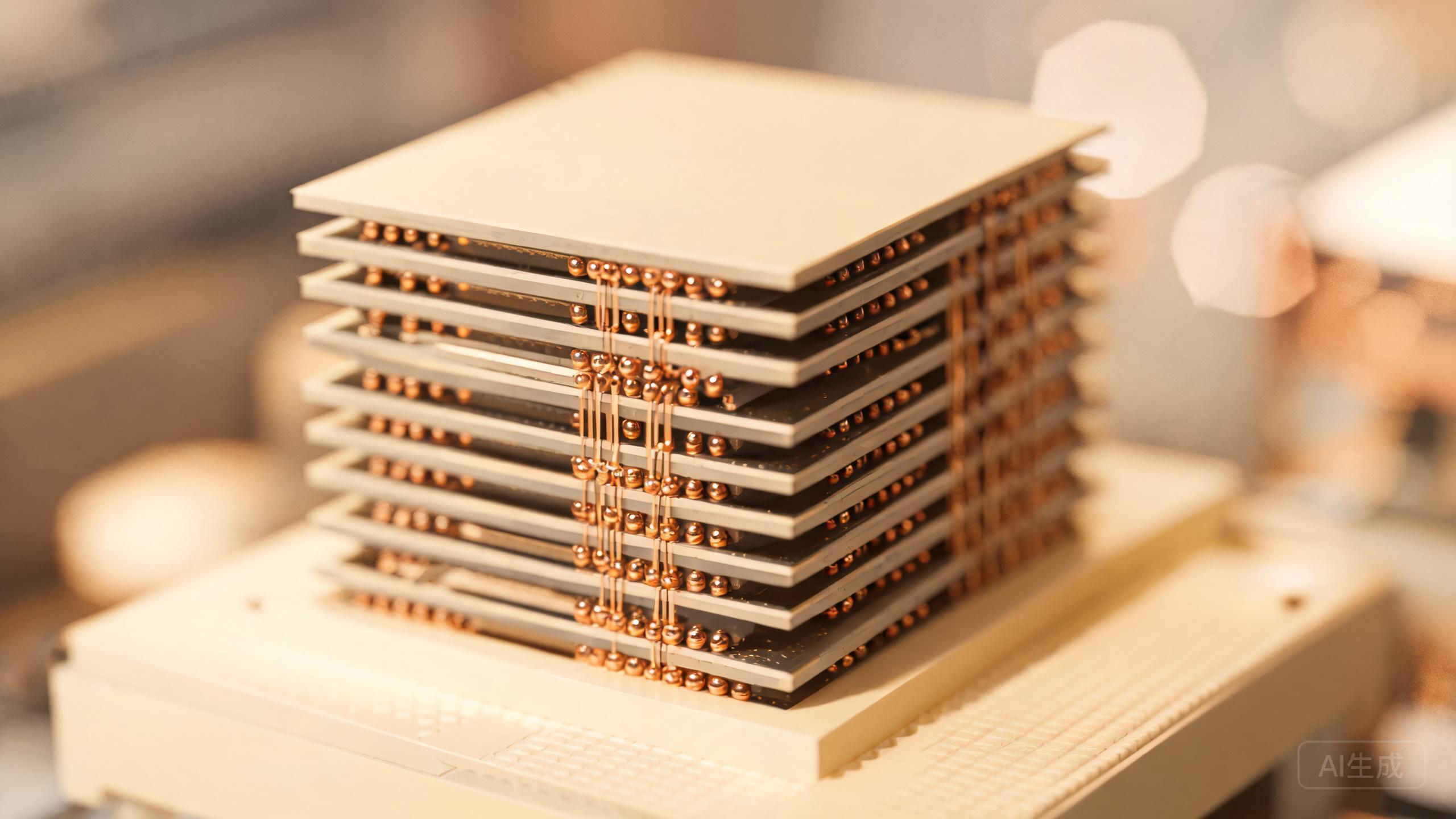
SK Hynix has started volume shipments of 16-high HBM4 stacks, pushing the memory industry's stacking roadmap beyond the twelve-layer generations that defined HBM3E. Each stack carries 48GB and connects through a 2048-bit interface, with pin speeds around 8 gigabits per second and per-stack bandwidth approaching two terabytes per second. The first shipments are destined for NVIDIA's Rubin platform, with AMD's MI450 program following later in the qualification cycle.
The most significant architectural change is not the
The most significant architectural change is not the layer count but the base die. HBM4 moves the logic layer from a conventional DRAM process to a foundry-built die manufactured by TSMC, allowing the memory to handle more complex testing, power management, and signal conditioning. That division of labor gives SK Hynix access to advanced logic without building it, but it also creates a new dependency on foundry allocation and on the interface design rules that customers expect.
SK Hynix: Stacking 16 dies reliably is a packaging
Stacking 16 dies reliably is a packaging problem before it is a lithography problem. SK Hynix continues to use MR-MUF, a molded underfill process that fills the gaps between dies in a single step and dissipates heat through the mold compound. The alternative, thermal compression with non-conductive film, offers finer pitch control but is slower and more prone to voids as stack height increases. Yield at 16-high remains the single largest determinant of HBM4 cost, and the company has spent the past two years tuning warpage control, wafer thinning, and known-good-die screening.
Capacity is being added at the M15X fab in?
Capacity is being added at the M15X fab in Cheongju and the Yongin cluster, but neither facility can relieve the shortage quickly. Industry estimates suggest HBM4 output is effectively sold out through 2027, and contract prices carry a premium several times that of commodity DRAM. SK Hynix is also allocating more wafer capacity to HBM at the expense of conventional DDR5, which tightens supply in the server memory market and contributes to the broader cost inflation in AI infrastructure.
Competition is closing in
Competition is closing in. Samsung is shipping 12-high HBM4 with its own foundry base die, and Micron has qualified 12-high stacks at major customers. SK Hynix's advantage rests on stacking maturity and its early relationship with NVIDIA, not on an unassailable process lead. The strategic conclusion is that memory has become a co-design discipline: the companies that win will be those that can align DRAM process, base-die logic, and customer packaging roadmaps years before a platform launches.
Key Takeaways
- SK Hynix continues to push boundaries in memory architecture.
- The development addresses fundamental physical limitations in semiconductor scaling.
- Commercial viability will depend on yield stability and supply chain integration.