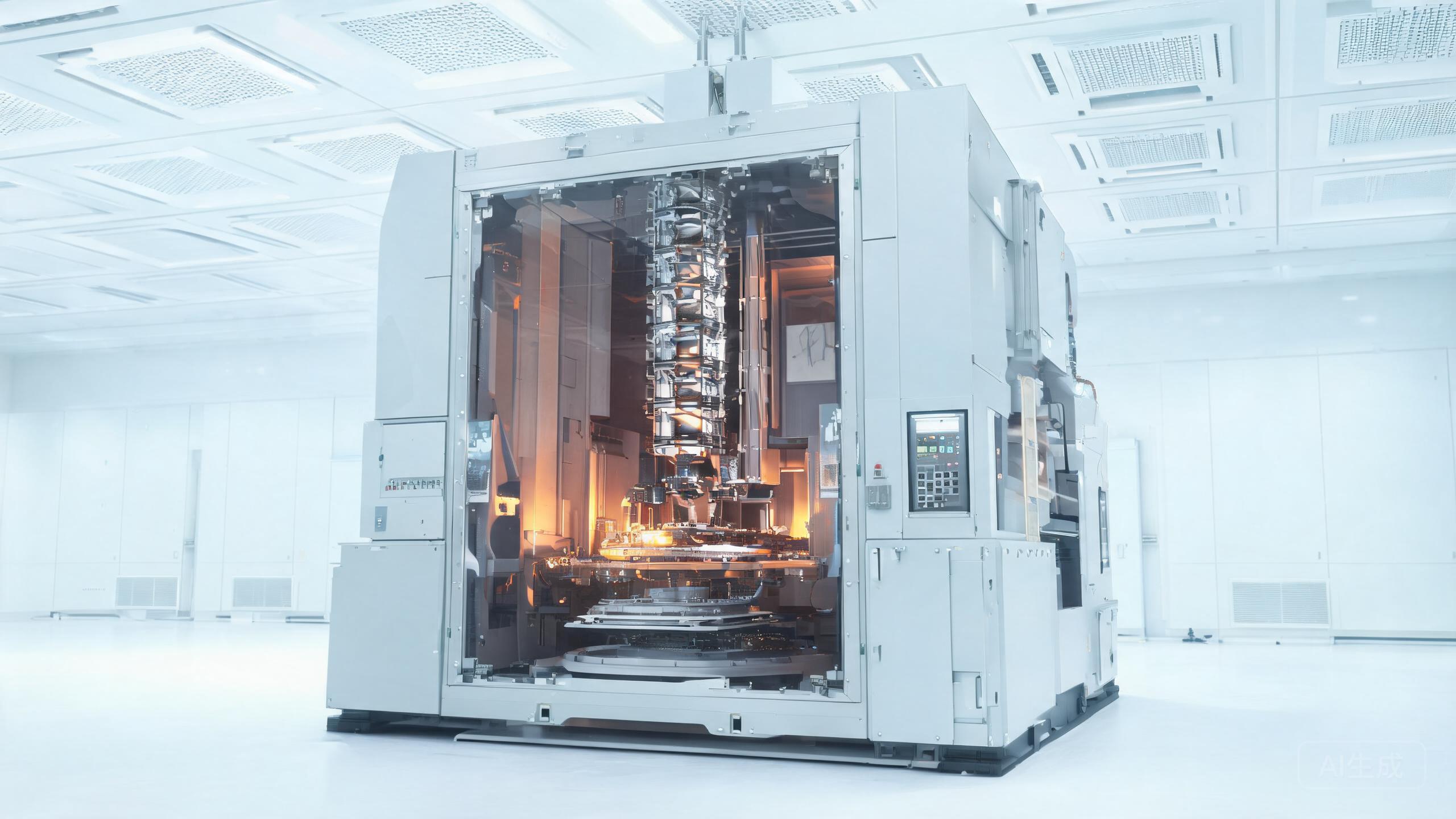
ASML has delivered another batch of EXE:5200 High-NA EUV systems to logic and memory customers, and the company says field data now shows sustained throughput above 200 wafers per hour on production patterns. That figure matters because it moves High-NA from an engineering demonstration into a tool that fabs can justify on cost per layer rather than on resolution alone.
High-NA lithography increases numerical aperture from 0
High-NA lithography increases numerical aperture from 0.33 to 0.55, shrinking the printable half-pitch from roughly 13nm to 8nm. The optics are larger, the mirror angles steeper, and the exposure field is half the size of a standard scanner field, which means many designs must be stitched from two exposures. Those tradeoffs initially limited the technology to a narrow set of critical layers. Better dose control, improved mask handling, and a more stable light source have now narrowed the productivity gap with conventional EUV.
ASML: The first production use is expected at
The first production use is expected at Intel's 14A node, where High-NA is paired with backside power delivery, and at Samsung and TSMC nodes in the 2028 to 2029 window. Memory makers are also evaluating the tool for 1-delta DRAM and for the capacitor layers that have become harder to pattern as cell density rises. Each additional adopter improves the installed base and gives ASML more field data to refine service and uptime models, a virtuous cycle that the company's competitors have not been able to replicate.
The cost picture remains sobering?
The cost picture remains sobering. A single High-NA scanner can exceed 350 million euros, and the surrounding mask infrastructure, resist chemistry, and metrology must be upgraded as well. Fabs are therefore introducing the tool selectively, using it where a layer benefits from smaller features and keeping conventional EUV for less critical levels. This hybrid approach reduces risk but complicates scheduling and fab layout, particularly in facilities that were designed around a single scanner footprint.
Beyond High-NA, ASML is studying a 0
Beyond High-NA, ASML is studying a 0.75 numerical aperture generation that would require another complete optical redesign. That work is still research, and the practical question for the rest of the decade is whether High-NA adoption broadens fast enough to support the cost curve. Export controls and regional supply policies add a further layer of uncertainty, but the technical direction is now clear: the industry has committed to larger optics, smaller fields, and more expensive light.
Key Takeaways
- ASML continues to push boundaries in lithography equipment.
- The development addresses fundamental physical limitations in semiconductor scaling.
- Commercial viability will depend on yield stability and supply chain integration.