What follows is a closer look at tsmc's panel-level packaging pilot line signals the end of the 300mm cowos monopoly — not as a product announcement, but as an engineering story with real consequences for the semiconductor supply chain.
TSMC has commissioned a pilot line for CoPoS, its
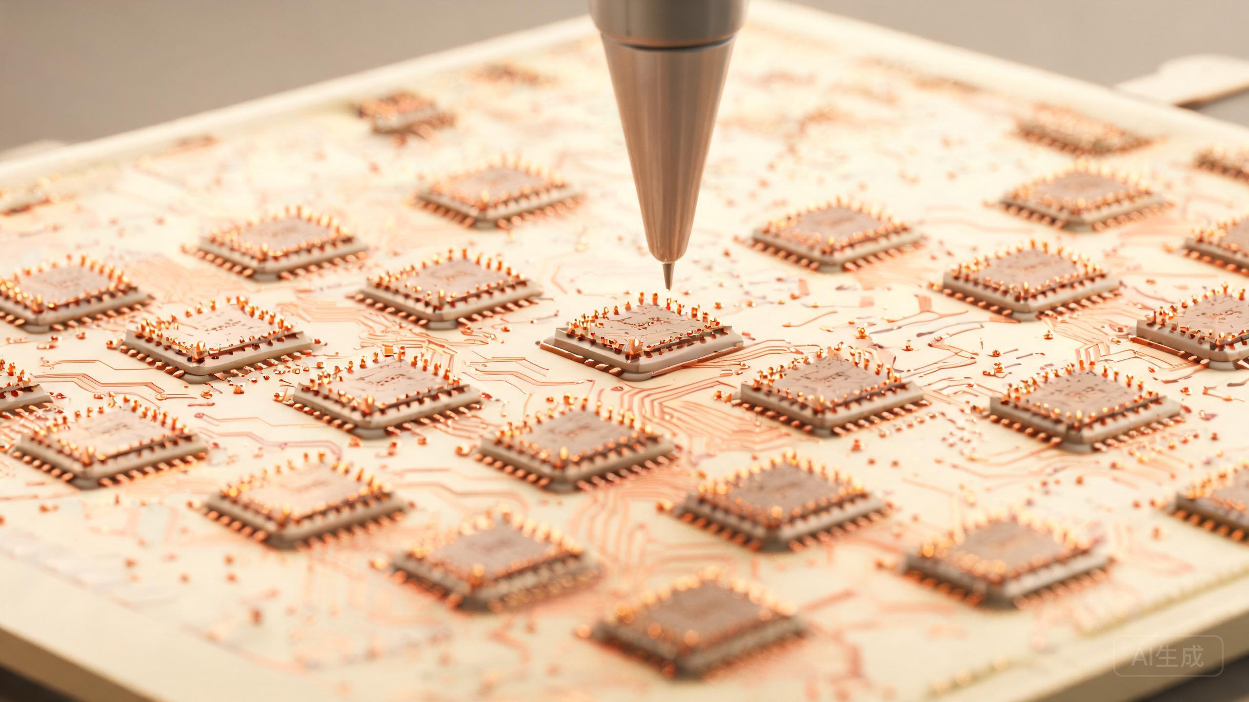
TSMC has commissioned a pilot line for CoPoS, its panel-level packaging platform, marking the first serious move by a leading-edge foundry away from round 300mm wafers as the base for AI chip assembly. The line packages chiplets on large rectangular panels using a glass carrier, then transfers the reconstituted panel to an organic substrate for board assembly.
The economic logic is straightforward
The economic logic is straightforward. A round wafer wastes substantial area at its edge, and the largest CoWoS interposers already consume most of a 300mm field. Rectangular panels improve area utilization and allow more packages per process pass, which lowers cost per unit area and increases output without building another cleanroom. Early estimates suggest a cost reduction of 40 to 60 percent for packages that fit the panel format, though those figures depend on yield and on how much of the existing CoWoS toolset can be reused.
TSMC: The engineering problems are concentrated in
The engineering problems are concentrated in mechanics rather than lithography. Panel warpage grows with size, and the mismatch in thermal expansion between glass, dielectric films, and copper redistribution layers becomes harder to control as dimensions increase. Fine-line RDL patterning on a panel requires new steppers or laser direct imaging tools, and die placement must maintain micron-level accuracy across a much larger field. Bonding and debonding the glass carrier adds steps that can introduce particles and stress.
TSMC is not alone in pursuing panels?
TSMC is not alone in pursuing panels. OSATs such as Amkor and ASE have panel-level programs, and equipment suppliers are developing adapted coaters, developers, and inspection systems. What TSMC brings is the ability to co-optimize packaging with its own front-end nodes and to guarantee a single qualification path for customers who already buy wafers from the same company. That integration is difficult for standalone assembly houses to match.
Mass production is not expected before
Mass production is not expected before 2028 or 2029, and the first use cases will likely be accelerators with repeated chiplet patterns rather than one-off designs. The strategic implication is that advanced packaging is becoming a foundry business in its own right. If panels deliver the projected cost curve, the constraint that has limited AI accelerator output for three years will ease, and packaging will stop being the hidden tax on every model deployment.